Notice
Perovskite’s time to shine in display technology [Nature Index 2024]
Writer 관리자
Date 24-12-13 21:15
Read 961
Perovskite’s time to shine in display technology
Breakthroughs in the fabrication of tiny perovskite crystals are opening opportunities for a new generation of displays with superior efficiency and colour fidelity.
Perovskite’s time to shine in display technology, https://www.nature.com/articles/d42473-024-00311-z
Nature Index 2024 Materials Science: https://www.nature.com/collections/materials-science-index-2024
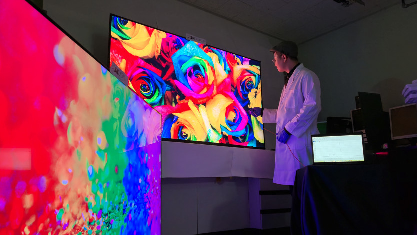
Television displays based on perovskite nanocrystals, shown here at SN Display in South Korea, exhibit excellent colour properties. Credit: SN Display
Intense competition in the display sector over the past decade has spawned a proliferation of technologies — from liquid-crystal displays (LCDs) through to organic light-emitting diode (OLED) and quantum-dot LED displays. The field is evolving rapidly, with refinements to advanced material technologies creating brighter, more vibrant, long-lasting and cheaper display panels.
As display makers push the limits of their technologies, the bar has been set so high that new technologies need to be truly groundbreaking.
Enter perovskite nanocrystals (PeNCs).
Halide perovskites have been studied for years as a low-cost, versatile material for catalysts, sensors, solar cells, LEDs and other optoelectronic devices. Halide perovskite materials are a class of compounds with a characteristic crystal structure and the general chemical formula ABX₃, where A can be a large organic or metal cation, B is typically a smaller metal ion, and X is a halide ion (such as chloride, bromide or iodide) with a negative charge.
That simple chemical formula gives rise to a highly uniform cubic crystal structure. Yet it also belies an enormous variety of possible atomic combinations, each resulting in a mineral crystal with unique properties, including the emission of light.
“I became fascinated with perovskites the first time I saw the luminescence from a perovskite emitter,” recalls Tae-Woo Lee, head of the display technology company SN Display based in Seoul, South Korea. “The purity of the colours was stunning — I had never seen anything like it. From that moment, my goal has been to commercialize perovskites as the foundation for next-generation display technology.”
Bulk to nanocrystals
Perovskites are best known for their use in next-generation solar cells. In solar cells, a perovskite absorbs light energy to create an exciton — a quasiparticle consisting of an electron and a hole — that rapidly breaks up. The electron and hole are then captured at the electrodes to generate an electric current.
However, this rapid dissociation of excitons into electrons and holes, which makes perovskites excellent for solar cells, hinders them from emitting light. “This intrinsic perovskite property has limited their use for displays despite their wonderful emission quality,” says Lee.
The breakthrough came when Lee’s team produced perovskite as nanoscale crystals. Until then, perovskites had primarily been fabricated as large-grain polycrystalline films, mainly for solar cells and other optoelectronic applications.
“At particle sizes of just about 10 nanometres, or little bit larger than the exciton Bohr diameter, all of sudden we could get bright emission at room temperature, with an electroluminescence efficiency comparable to that of today’s OLEDs,” says Lee.
That discovery, which was patented in 20141,2,3 and published in 20154, laid the foundation for display technology based on perovskites that promises to outperform other display technologies.

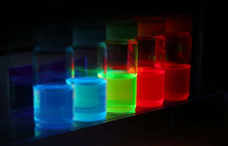
Nanocrystals of perovskites in solution emit light of different colours depending on the chemical compositions of the nanocrystals. Credit: SN Display
Light like no other
Arguably the most enticing feature of PeNCs is the purity of their colour. Light emission from organic emitters and quantum dots is spread across the colour spectrum, measured in the spectral width of light wavelengths emitted. Typical OLEDs and quantum-dot LEDs have a spectral width of about 50 nanometres and 35 nanometres, respectively. In contrast, PeNCs can reach as narrow as 20 nanometres — the narrowest reported for any nanocrystal. This unparalleled sharpness in emission grants PeNCs their remarkable true-to-life colour quality, making them capable of achieving 100% coverage of the Rec. 2020 colour gamut.“
“Conventional inorganic quantum dots can’t achieve the narrow spectral width that our PeNCs can,” notes Lee.
The current premium display market primarily features two types of displays: colour-conversion displays (such as LCDs backlit by LEDs with a quantum-dot colour-conversion layer or OLEDs using quantum-dot colour-conversion pixels) and self-emissive displays, such as OLEDs.
“In this nanocrystal-size regime beyond quantum confinement, where high quantum efficiency and narrow emission spectra are retained, perovskites exhibit exceptional optical properties, making them ideal for colour-conversion films when paired with conventional blue-light LED backlights,” says Lee. “We’ve fabricated backlit displays using the PeNC films as highly efficient colour-conversion layers up to 75 inches in size, with high brightness and exceptional colour purity and a wide colour gamut.”
Since the initial discovery, Lee’s team has been working on developing an efficient way to make PeNCs in quantity.
“We’ve developed a high-yield, low-cost, room-temperature synthesis method that allows us to produce large-area films of high-quality PeNCs very efficiently,” says Lee. “This method doesn’t require their extreme synthesis conditions such as high temperatures —about 300°C — usually required for conventional inorganic quantum dots.”
Lee’s team in SN Display is now working with industry partners to commercialize this perovskite nanocrystal technology for displays. “We’re collaborating with leading companies like Samsung and Hyundai to advance this technology and explore its potential for future commercial products.”
Nanocrystal arrays
To meet industry demands, SN Display is developing a PeNC array tailored for high-resolution augmented reality (AR) and virtual reality (VR) displays exceeding 3,000 pixels per inch.
By modifying the surface chemistry of nanocrystals with specialized resins and various ligands, and with about a ten-fold higher absorption coefficient than conventional inorganic quantum dots, their PeNC ink supports high-resolution patterning techniques such as photolithography, inkjet printing and transfer patterning. The array features ultrasmall pixels (2–3 micrometres) arranged to create prototypes of colour-enhanced micro OLED/LED devices, enabling effective blue-light absorption and conversion with a thickness of just 1–2 micrometres, which is challenging for conventional inorganic quantum dots. This innovative approach promises to reduce the cost of next-generation displays while enhancing the colour purity of current display technologies.
In addition to his role at SN Display, Lee is a professor at Seoul National University. He has a strong research team to continue developing pixelized PeNC array technology for AR/VR and collaborating with Meta Platforms, Inc.
Nanocrystals for LEDs
While the use of PeNCs for back-lit displays is showing a lot of promise, self-emissive displays are considered the ideal display technology, as they offer higher contrast and energy efficiency across displays, lighting and photonic devices.
Furthermore, this technology should deliver a full gamut of true-to-life colours with high efficiency, be easily fabricated in micrometre-scale pixels, have long-term stability, and be produced efficiently at low cost using common materials under mild conditions. With PeNCs, this ideal is now closer than ever.
In 2022, Lee’s team published a paper in Nature5 detailing an electroluminescent device fabricated using an in situ core–shell strategy. It achieved a record external quantum efficiency, an impressive brightness, and an extended device lifetime — an improvement of nearly a 100-fold over the previous lifetime record in the field.
“We’re in the process of commercializing a self-emissive electroluminescent pixel technology based on our PeNC platform for self-emissive displays,” says Lee.
Lee is excited about the potential of using PeNCs as light source for various applications. “Our technology can provide solutions for many different areas,” says Lee. “Beyond the mass display market, it is also very suitable for other applications such as light sources for AR/VR displays, medical displays, educational displays, flexible and stretchable displays, vehicles and watches.”
But it is the area of displays that he sees the most promise. “Our technology is cheap, even though it has the best colour quality reported in this field,” says Lee. “We believe it will be the next high-performance display technology, with outstanding colours.”
References
-
Lee, T.-W. et al. Patent No. WO2016072805A1, Priority date: 6 November 2014
-
Lee, T.-W. et al. Patent No. WO2016072803A1, Priority date: 6 November 2014
-
Lee, T.-W. et al. Patent No. WO2016072806A2, Priority date: 6 November 2014
-
Cho, H. et al. Science 350, 1222–1225 (2015).
-
Kim, J. S. et al. Nature 611, 688–694 (2022).
출처: Perovskite’s time to shine in display technology, https://www.nature.com/articles/d42473-024-00311-z
Files
- SNDISPLAY_Perovskites time to shine in display technology_Nature Index 2024 Material Science.pdf (205.8K) Download


